For customers who develop and manufacture semiconductor wafers such as SiC (silicon carbide), GaN (gallium nitride) and Ga2O3 (gallium oxide), a major issue is how to inspect the quality of the semiconductor wafer crystals they have created. Generally, defect density is optically inspected, but semiconductor wafer crystal quality is affected not only by defect density but also by dopant concentration and other factors. Thus, it is necessary to conduct multifaceted quality inspections in parallel with optical quality inspection.
We have put into practical application a proprietary technology invented by Tohoku University called the HS-CMR method, an inspection method for semiconductor wafer crystal quality using an electrical approach. Our HS-CMR method enables inspecting the crystal quality of semiconductor wafers that cannot be seen with optical inspection methods.
In addition to manufacturing and sales of semiconductor wafer testers using the HS-CMR method, we also offer contracted services for quality inspection of semiconductor wafers using the HS-CMR method. We make it easy for customers to utilize the HS-CMR method by performing quality inspections on semiconductor wafers received from customers. We can handle as little as one piece of semiconductor wafer, so please feel free to contact us for more information.

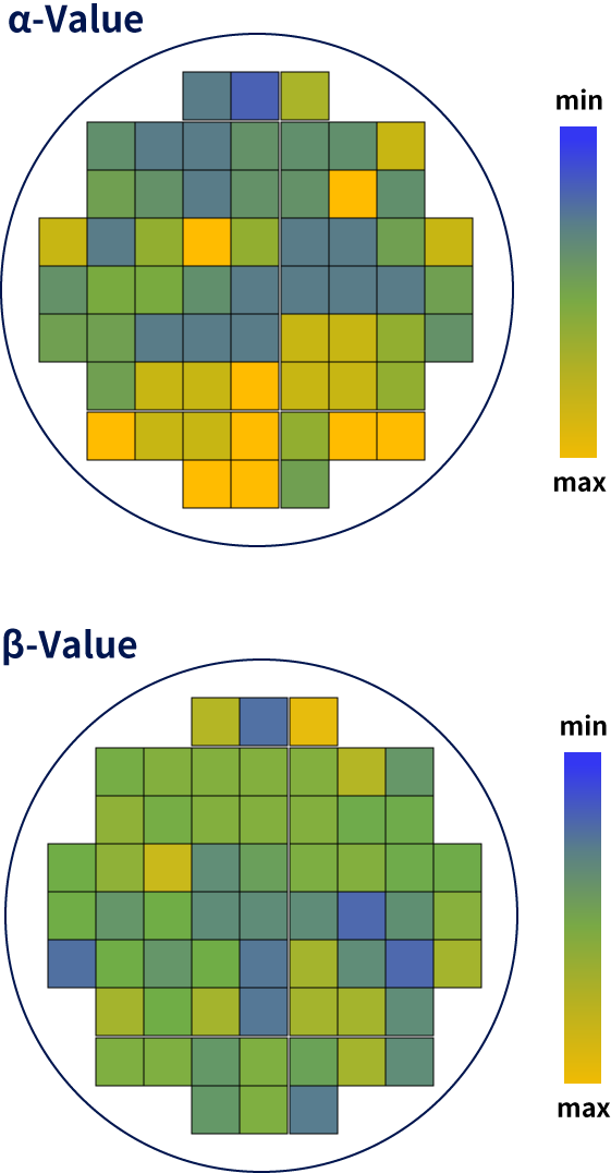
The α and β values are displayed by color mapping, allowing
you to visually capture the distribution of crystal quality.

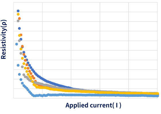
By graphing the actual measurements at each measurement point and comparing them with other measurement points, the characteristics of the wafer surface and interior can be captured.
Quality inspection is possible even on pre-polished as-sliced wafers which cannot be inspected with optical inspection methods!
Data correlating to the number of etch pits can be obtained for polished wafers without performing alkaline etching required by optical inspection methods!
Because testing can be performed without advanced pretreatment, test results can be returned in about one week after receiving the sample!
In the development of compound semiconductor ingots, easy evaluation of crystal quality has made it possible to quickly provide data feedback to crystal growth experiments and shorten the experiment cycle. (Power semiconductor crystal development)
Two ingots we received from a customer were sliced under the same conditions, but one was warped while the other was not. We had trouble handling this, but measurement using the HS-CMR method revealed that this defect was due to crystal quality. (Ingot processing materials manufacturer)


|
STEP1 |
Please contact us using the inquiry form below. |
|---|---|
|
STEP2 |
We will provide a quotation after discussing the overview of the samples and measurement details, etc. |
|
STEP3 |
Please send us the order form and samples. |
|
STEP4 |
Measurement and analysis can be performed in as little as one week after receiving the samples. |
|
STEP5 |
We will send you the measurement report, and return your samples. |